ReRAM Market: Technological Advancements Strengthening High-Performance Memory Applications
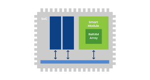
The physical scaling of non-volatile memory technologies depends on seamless integration with standard semiconductor fabrication processes without introducing complex thermal cycles or non-standard chemical contamination. Resistive random-access memory stands out in the memory landscape because its metal-insulator-metal (MIM) device stack can be processed entirely within the Backend-of-Line (BEOL) interconnect layers. Analyzing ongoing industry movements using comprehensive ReRAM Market trends showcases how leading foundries leverage materials like hafnium oxide, tantalum oxide, and titanium nitride to fabricate highly uniform filamentary switching cells. Depositing these materials between metal layers allows chip makers to place dense non-volatile memory directly above logic circuitry, saving valuable silicon real estate and shortening interconnect wire lengths.
Material scientists continue to optimize the switching layer stoichiometry to resolve historical variations in write endurance and resistance retention across wide temperature ranges. Inserting oxygen-vacancy reservoir layers or bilayer dielectric structures allows engineers to constrain conductive filament formation to deterministic paths, reducing device-to-device variability. Advanced atomic layer deposition (ALD) techniques enable nanometer-level control over dielectric layer thickness, which directly stabilizes threshold switching voltages. Concurrently, selector technology development—utilizing ovonic threshold switches (OTS) or volatile conductive-bridging layers—is crucial for enabling dense 3D vertical crossbar structures (VReRAM). These physical and material breakthroughs are establishing resistive RAM as a highly scalable alternative for future semiconductor manufacturing nodes below 10nm.
Frequently Asked Questions
-
What is the function of an oxygen-vacancy reservoir layer in a ReRAM cell? An oxygen-vacancy reservoir layer acts as a source and sink for oxygen ions during switching operations, stabilizing conductive filament formation and improving overall device endurance and retention consistency.
-
Why is Backend-of-Line (BEOL) integration an advantage for semiconductor foundries? BEOL integration means the memory stack is deposited on top of the silicon wafer after the main logic transistors are built. This avoids high-temperature steps that could damage logic circuits and allows memory to be placed directly above logic cores.
➤➤➤Explore MRFR’s Related Ongoing Coverage In Semiconductor Industry:
Musical Instrument Insurance Market
Next Generation 3D Display Market
Non Contact Infrared Thermometer Market
Non Volatile Dual In Line Memory Module Market
Powder Bed Fusion Process 3D Printer Market
Property Casualty Reinsurance Market
Categorie
Leggi tutto
Netflix, a global leader in digital entertainment, has announced its upcoming slate of original programming in Latin America, with a focus on Argentina. Among these projects is the highly anticipated series "Puerta 7," a compelling drama exploring the complex world of soccer fan groups, known locally as barra bravas. Set to be produced by Argentina’s renowned Pol-ka, "Puerta 7" promises...

The phrase “getting queerbaited by Marvel is like losing chess to a dog” perfectly captures the frustration many fans feel. Often, Marvel only offers vague hints or small tokens of LGBTQ+ representation, leaving us wondering if there’s more beneath the surface. So, while the latest buzz around Marvel Rivals deserves a cautious eye, it’s still an intriguing topic to...
Netflix is set to unleash an adorable yet formidable protagonist onto screens worldwide through a groundbreaking animated interactive experience. This diminutive, fluffy warrior—sporting a signature pink bow—is far from your typical feline companion. The series centers on a determined character who combines extraordinary power, instinctive combat skills, and stylish gear to conquer...
A fresh ensemble navigates a perplexing parallel existence in this upcoming Netflix series. Inspired by classic tales of societal breakdown, the story thrusts a teenage community into an uncanny replica of their home, devoid of adults. Marc Webb brings his directorial vision as an executive producer, with Chris Keyser penning the ten-episode arc. Leading the cast is Kathryn Newton as Allie, a...
Netflix users across the globe will experience some exclusive benefits not available to viewers in the United States and Canada. Notably, the Netflix version of “Star Trek: Discovery” will feature episodes with Klingon subtitles, enhancing accessibility for fans interested in the series' unique language elements. Additionally, Netflix has released a trailer prominently displaying...